About Technology
Packaging (Assembly)/COB
Do you have worries/difficulties relating with packaging (Assembly)/COB? Would you please click “blue fonts” which you have interested?
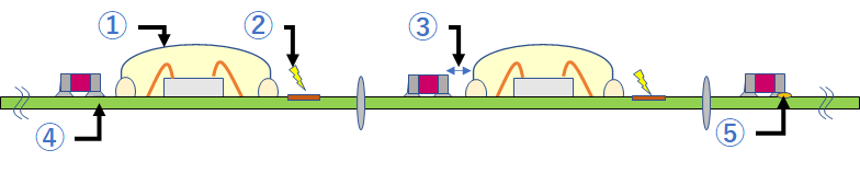
1.Introduction of applied form control with quantitative application control auto inspection by resin lot unit
Dispense equipment is setting application condition to make it as the requested size, along with viscosity, etc., that could be changed due to resin lot.
Processing Flow
1.Part packaging -> 2.Forming Dam -> 3.Forming spheric lens
*Processing of mid layer with different sealing material from lens material up to height of internal wire.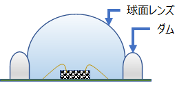
Visual inspection equipment has auto judge of application form with image.
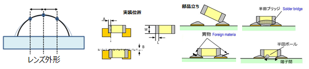
Inspection items
Depiction frame height/Roundness degree/Position accuracy, Bottom surface diameter, Lens frame height/form/position accuracy, overflowed resin, depiction frame foreign substance, lens foreign substance, dirt on top of packaging, peripheral crack
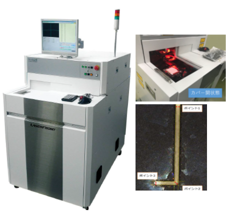
2.Laser trimming of Thick film resistor wiring
Function trimmer with innovated high performance and high function. Equipment to compensate variation of out put value with laser trimming to control circuit. Use would be for processing of automotive electronics part, module packaging, hybrid IC various types of sensor (Electric current, voltage, etc.,) LED lighting brightness adjustment thick film resistor, Thin film resistor, Metal foil resister, etc.,
TLF SL 432R series
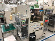
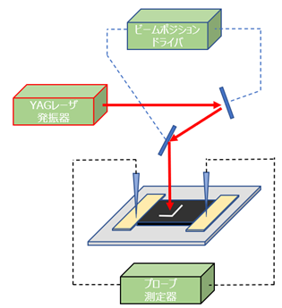
Equipment system (Figure)
3.Capable to install various types of chip part and IC
Dispenser Supplementary material
DAM forming
Lens forming
4.Organic Board, Ceramic Board, Metal Board
We have production actual results for Organic/Ceramic/Metal Board
| Mass Production/ Pilot | products | Board | Package method |
|---|---|---|---|
| Mass Production | Si Chip | Lead frame | DB-WB-MP-TF |
| Mass Production | Si Chip | Map Galaeppo (FR4) | DB-WB-MP-MAP piece |
| Mass Production | Sensor, ASIC, Amp | hollow plastic mold | DB-WB-DP-Lid Installed –TP |
| Mass Production | MEMS | Ceramics | DB-WB-DP-Lid Installed |
| Mass Production | thermoelectric element | Aluminum nitride | Solder printing- DB-Pulse heat-Cold and heat test |
| Mass Production | Blue-light LED COB | Fine Ceramics | COB(DP Phosphor)-SMT |
| Mass Production | LED SMD Packaging | Aluminum | SMT |
| Mass Production | Voice IC+ LED+CR | Galaeppo(FR4) | SMT |
| Mass Production | Red-light LED | Ceramics | SMT-DB-WB-DP Lens (-wire trimming) |
| Mass Production | Red-Light LED | Galaeppo(FR4) | SMT-DB-WB-DP Lens-Board piece |
| Mass Production | UV-LED | Aluminum nitride | DB-WB-DPLens |
| Pilot | Laser Module | Ceramics | DB-WB-DPLens |
| Pilot | Infrared rays module | Aluminum | DB-WB-DP Lens |
| Pilot | Photodiode | Galaeppo(FR4) | DB-WB-Clear DB-MAP piece |
(Process code) DB: Dice Bonding, WB:Wire Bonding, MP:Mold press, TF: Lead process, DP: Dispenser application, SMT :Surface packaging line
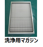
5.Introduction of Direct path cleaner
Cleaning residue hidden in concentrated parts can be removed.
In-line equipment
- Solder screen printing
- Solder printing auto inspection (SPI)
- Chip mounting equipment
- Reflow/li>
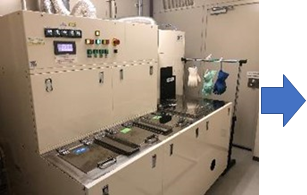
Flux cleaner
Stable cleaning performance is achieved by fixture design that takes liquid flow optimization into consideration.
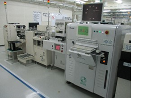
Auto Visual Inspection Equipment (AOI)
Don’t you have worries/difficulties like the followings?
-
Looking for packaging manufacturer that can correspond small pilot and small production!
- -> Please consult to us, we will propose quotation.
-
Looking for manufacturer that can develop together because you need a new technology!
- ⇒ We have experience of general semiconductor Assembly and packaging of small type such of MEMS. We are capable to develop together with you by having conversation of future prospect./li>
-
"You would like to start initial prototype within Japan and implement mass production in oversea"
- -> We have oversea mass production plant in Bintan Island (Indonesia) where close to Singapore (Hub of world).
Please contact to the following sales person in charge. We will provide you solution.
Phone#: 81.983.33.5913 Persons in charge :Yamamura & Ota